- 您现在的位置:买卖IC网 > Sheet目录3862 > PIC18F66J15-I/PT (Microchip Technology)IC PIC MCU FLASH 48KX16 64TQFP
PIC18F87J10 FAMILY
DS39663F-page 34
2009 Microchip Technology Inc.
3.5
Internal Oscillator Block
The PIC18F87J10 family of devices includes an inter-
nal oscillator source (INTRC) which provides a nominal
31 kHz output. The INTRC is enabled on device
power-up and clocks the device during its configuration
cycle until it enters operating mode. INTRC is also
enabled if it is selected as the device clock source or if
any of the following are enabled:
Fail-Safe Clock Monitor
Watchdog Timer
Two-Speed Start-up
These features are discussed in greater detail in
The INTRC can also be optionally configured as the
default clock source on device start-up by setting the
FOSC2 Configuration bit. This is discussed in
3.6
Clock Sources and
Oscillator Switching
The PIC18F87J10 family includes a feature that allows
the device clock source to be switched from the main
oscillator to an alternate clock source. PIC18F87J10
family devices offer two alternate clock sources. When
an alternate clock source is enabled, the various
power-managed operating modes are available.
Essentially, there are three clock sources for these
devices:
Primary oscillators
Secondary oscillators
Internal oscillator
The primary oscillators include the External Crystal
and Resonator modes and the External Clock modes.
The particular mode is defined by the FOSC<2:0>
Configuration bits. The details of these modes are
covered earlier in this chapter.
The secondary oscillators are those external sources
not connected to the OSC1 or OSC2 pins. These
sources may continue to operate even after the
controller is placed in a power-managed mode.
PIC18F87J10 family devices offer the Timer1 oscillator
as a secondary oscillator. This oscillator, in all
power-managed modes, is often the time base for
functions such as a real-time clock.
Most often, a 32.768 kHz watch crystal is connected
between the RC0/T1OSO/T13CKI and RC1/T1OSI
pins. Loading capacitors are also connected from each
pin to ground.
The Timer1 oscillator is discussed in greater detail in
In addition to being a primary clock source, the internal
oscillator is available as a power-managed mode
clock source. The INTRC source is also used as the
clock source for several special features, such as the
WDT and Fail-Safe Clock Monitor.
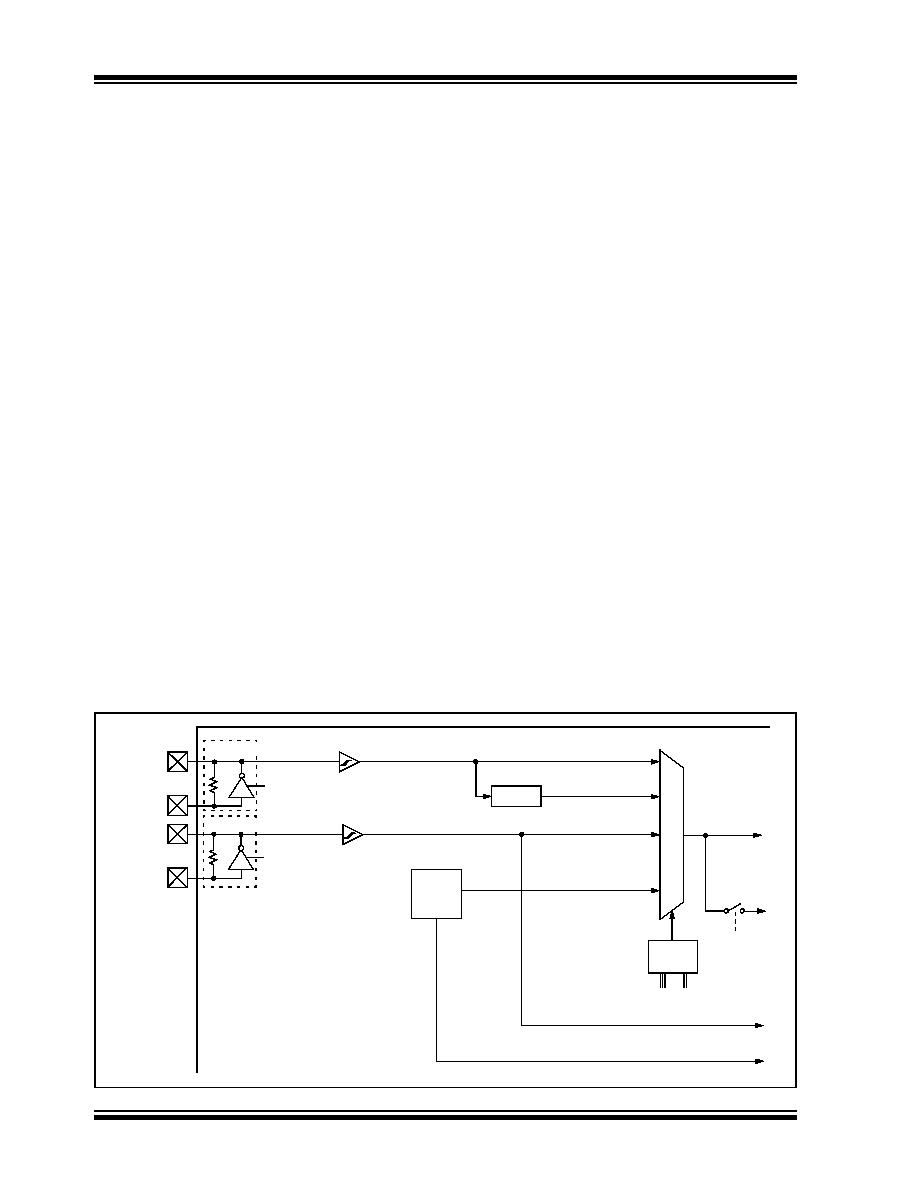
The clock sources for the PIC18F87J10 family devices
are shown in Figure 3-5. See Section 24.0 “Special
Features of the CPU” for Configuration register details.
FIGURE 3-5:
PIC18F87J10 FAMILY CLOCK DIAGRAM
PIC18F87J10 Family
4 x PLL
FOSC<2:0>
T1OSCEN
Enable
Oscillator
T1OSO
T1OSI
Clock Source Option
for Other Modules
OSC1
OSC2
Sleep
HSPLL, ECPLL
HS, EC
T1OSC
CPU
Peripherals
IDLEN
MUX
INTRC
Source
WDT, PWRT, FSCM
Internal Oscillator
Clock
Control
OSCCON<1:0>
and Two-Speed Start-up
Primary Oscillator
Secondary Oscillator
发布紧急采购,3分钟左右您将得到回复。
相关PDF资料
PIC24FV32KA302-I/SO
MCU 32KB FLASH 2KB RAM 28-SOIC
PIC24HJ64GP204-I/ML
IC PIC MCU FLASH 64K 44-QFN
SFW27R-2STE1
SFW27R-2STE1-FFC/FPC CONN
PIC24F16KA302-I/SP
MCU 16KB FLASH 2KB RAM 28-SPDIP
PIC18LF45J11-I/ML
IC PIC MCU FLASH 32K 2V 44-QFN
PIC24F32KA302-I/SO
MCU 32KB FLASH 2KB RAM 28-SOIC
PIC32MX120F032D-I/TL
IC MCU 32BIT 32KB FLASH 44-VTLA
PIC18F45J11-I/ML
IC PIC MCU FLASH 32K 2V 44-QFN
相关代理商/技术参数
PIC18F66J15T-I/PT
功能描述:8位微控制器 -MCU 96 KB FL 4 KB RAM RoHS:否 制造商:Silicon Labs 核心:8051 处理器系列:C8051F39x 数据总线宽度:8 bit 最大时钟频率:50 MHz 程序存储器大小:16 KB 数据 RAM 大小:1 KB 片上 ADC:Yes 工作电源电压:1.8 V to 3.6 V 工作温度范围:- 40 C to + 105 C 封装 / 箱体:QFN-20 安装风格:SMD/SMT
PIC18F66J16-I/PT
功能描述:8位微控制器 -MCU 96KB FL 3936b RAM 10 MIPS 51 I/O RoHS:否 制造商:Silicon Labs 核心:8051 处理器系列:C8051F39x 数据总线宽度:8 bit 最大时钟频率:50 MHz 程序存储器大小:16 KB 数据 RAM 大小:1 KB 片上 ADC:Yes 工作电源电压:1.8 V to 3.6 V 工作温度范围:- 40 C to + 105 C 封装 / 箱体:QFN-20 安装风格:SMD/SMT
PIC18F66J16T-I/PT
功能描述:8位微控制器 -MCU 96KB Flash 3936 bytesRAM 51I/O RoHS:否 制造商:Silicon Labs 核心:8051 处理器系列:C8051F39x 数据总线宽度:8 bit 最大时钟频率:50 MHz 程序存储器大小:16 KB 数据 RAM 大小:1 KB 片上 ADC:Yes 工作电源电压:1.8 V to 3.6 V 工作温度范围:- 40 C to + 105 C 封装 / 箱体:QFN-20 安装风格:SMD/SMT
PIC18F66J50-I/PT
功能描述:8位微控制器 -MCU 64KB FLSH 3936Bs RAM USB 2.0 nanoWatt RoHS:否 制造商:Silicon Labs 核心:8051 处理器系列:C8051F39x 数据总线宽度:8 bit 最大时钟频率:50 MHz 程序存储器大小:16 KB 数据 RAM 大小:1 KB 片上 ADC:Yes 工作电源电压:1.8 V to 3.6 V 工作温度范围:- 40 C to + 105 C 封装 / 箱体:QFN-20 安装风格:SMD/SMT
PIC18F66J50T-I/PT
功能描述:8位微控制器 -MCU 64KB FLSH 3936Bs RAM USB 2.0 nanoWatt RoHS:否 制造商:Silicon Labs 核心:8051 处理器系列:C8051F39x 数据总线宽度:8 bit 最大时钟频率:50 MHz 程序存储器大小:16 KB 数据 RAM 大小:1 KB 片上 ADC:Yes 工作电源电压:1.8 V to 3.6 V 工作温度范围:- 40 C to + 105 C 封装 / 箱体:QFN-20 安装风格:SMD/SMT
PIC18F66J55-I/PT
功能描述:8位微控制器 -MCU 96KB FLSH 3936Bs RAM USB 2.0 nanoWatt RoHS:否 制造商:Silicon Labs 核心:8051 处理器系列:C8051F39x 数据总线宽度:8 bit 最大时钟频率:50 MHz 程序存储器大小:16 KB 数据 RAM 大小:1 KB 片上 ADC:Yes 工作电源电压:1.8 V to 3.6 V 工作温度范围:- 40 C to + 105 C 封装 / 箱体:QFN-20 安装风格:SMD/SMT
PIC18F66J55T-I/PT
功能描述:8位微控制器 -MCU 96KB FLSH 3936Bs RAM USB 2.0 nanoWatt RoHS:否 制造商:Silicon Labs 核心:8051 处理器系列:C8051F39x 数据总线宽度:8 bit 最大时钟频率:50 MHz 程序存储器大小:16 KB 数据 RAM 大小:1 KB 片上 ADC:Yes 工作电源电压:1.8 V to 3.6 V 工作温度范围:- 40 C to + 105 C 封装 / 箱体:QFN-20 安装风格:SMD/SMT
PIC18F66J60-I/PT
功能描述:8位微控制器 -MCU 64KB FL 12KB RAM 10BASE-T RoHS:否 制造商:Silicon Labs 核心:8051 处理器系列:C8051F39x 数据总线宽度:8 bit 最大时钟频率:50 MHz 程序存储器大小:16 KB 数据 RAM 大小:1 KB 片上 ADC:Yes 工作电源电压:1.8 V to 3.6 V 工作温度范围:- 40 C to + 105 C 封装 / 箱体:QFN-20 安装风格:SMD/SMT